
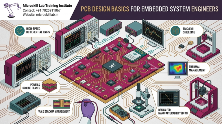
PCB design is the process of turning a circuit schematic into a manufacturable board layout that powers every embedded system, from a simple Arduino sensor node to an industrial control unit. For electronics students in Bangalore, learning PCB design basics means understanding schematic capture, component placement, copper routing, and design rule checks well enough to take a project from idea to a working prototype. This guide walks through the fundamentals every embedded hardware learner needs before their first tape-out.
Whether you are a final-year engineering student preparing for placements or a working professional pivoting into embedded hardware, the same core sequence applies: capture the schematic correctly, place components with layout constraints in mind, route copper cleanly, and verify everything against design rules before sending files to a fabrication house. We break down each of these stages below, with a Bangalore-specific view of tools, costs, and career outcomes.
⚡ Key Takeaways
- You will understand the full PCB design workflow, from schematic capture to fabrication-ready Gerber files.
- You will learn how embedded hardware decisions (microcontroller footprint, power rails, signal integrity) shape a good layout.
- You will compare KiCad and Altium Designer so you know which tool to learn first.
- You will see real Bangalore salary bands and hiring companies for PCB design engineers in 2026.
- You will get a clear view of course duration, fees, and batch options before enrolling.
- You will know which career roles open up after mastering circuit design and PCB layout.
What Is PCB Design in Embedded Systems?
PCB design is the discipline of converting an electronic circuit into a physical printed circuit board that connects a microcontroller, sensors, power regulators, and connectors through copper traces. In embedded systems specifically, the board is not just a support structure — it directly affects signal quality, thermal performance, and long-term reliability of the product.
Every embedded engineer who writes firmware eventually needs to understand the hardware it runs on. Our PCB Designing Programme → is built around this exact gap, taking electronics students from schematic basics to a fully routed, fabrication-ready board.
Schematic Design vs PCB Layout
Schematic design is the logical representation of a circuit — how components connect electrically, without any concern for physical placement. PCB layout is the physical realization of that schematic, where every component gets a footprint, a position, and copper traces that respect electrical and manufacturing rules.
Students often confuse the two skills. A correct schematic can still produce a poor board if routing ignores trace width, via placement, or ground plane continuity. Learning both stages together, as we teach in our workshops, prevents this common beginner mistake.
Key Components of an Embedded PCB
A typical embedded PCB includes several functional blocks that every student should recognise before their first layout attempt:
- Microcontroller or SoC (STM32, ESP32, PIC, AVR)
- Power regulation section (LDOs, buck converters, protection diodes)
- Crystal oscillator and decoupling capacitors
- Communication interfaces (UART, I2C, SPI, USB)
- Connectors, headers, and test points
- Ground and power planes for noise reduction
Understanding these blocks in a schematic makes the transition to layout far more intuitive, because you already know why each component exists on the board.
Many first-time learners skip straight to routing without mapping out these functional blocks first, which often leads to messy layouts and awkward trace crossings later. We encourage students to sketch a rough block diagram — power in, microcontroller core, sensor interfaces, output stage — before opening any layout software. This planning step, borrowed from professional embedded hardware design, saves hours of rework once routing begins.
Why PCB Design Matters for Electronics Students in Bangalore in 2026
Bangalore is home to one of India’s densest concentrations of embedded hardware companies, and demand for engineers who can move between firmware and PCB design keeps growing every year. Students who only learn to code microcontrollers, without understanding the board those chips sit on, limit their own career ceiling in this market.
Bangalore's Electronics and IoT Hardware Ecosystem
Electronic City, Whitefield, and Manyata Tech Park host a wide mix of embedded product companies, IoT startups, and global R&D centres that hire locally trained PCB design engineers. Karnataka’s electronics manufacturing push, supported by state IT/ITES policy, has widened the hiring pool for entry-level hardware roles beyond just the large multinational firms.
This means Bangalore-trained students get access to internships and junior design roles that many other Indian cities simply do not offer at the same scale. Our Embedded Systems Professional Programme → is designed with this local hiring landscape in mind.
Salary Benchmarks for PCB Design Engineers
Entry-level PCB design engineers in Bangalore typically start in the ₹3.5–6 LPA range, while engineers with 2–4 years of layout and signal integrity experience can move into the ₹6–12 LPA band, depending on the company and product complexity. These figures vary by employer and project scope, so students should treat them as indicative ranges rather than guarantees.
Specialised skills such as high-speed digital layout, RF board design, or multilayer stack-up expertise tend to command a premium over generalist PCB roles. Building this specialisation early, through structured coursework and live projects, gives students a measurable edge when they enter the job market.
Core PCB Design Workflow: From Schematic to Fabrication
A professional PCB design workflow follows a consistent sequence regardless of which software tool you use. Learning this sequence well matters more than memorising any single tool’s interface, because the underlying logic transfers across KiCad, Altium, Eagle, or any other package you encounter later in your career.
Schematic Capture and Component Selection
The workflow begins with schematic capture, where you place symbols for every component and wire them according to the circuit’s logic. At this stage, component selection decisions — package type, voltage rating, tolerance — directly determine how easy or difficult the layout stage will be later.
We teach students to build a habit of checking datasheets for footprint and power requirements before placing any component in the schematic. This single habit prevents most of the rework that beginner designers run into during layout.
Layout, Routing, and Design Rule Checks
Once the schematic is complete and components are assigned footprints, the layout stage begins with placement, followed by copper routing between pads. Design rule checks (DRC) then verify that trace widths, clearances, and via sizes meet the fabrication house’s manufacturing capabilities.
Common beginner tools and techniques covered in this stage include:
- Grid-based and free-angle routing techniques
- Ground plane pours and thermal relief settings
- Via stitching for multilayer boards
- Design rule check (DRC) and electrical rule check (ERC) configuration
- Gerber and drill file generation for fabrication
Skipping DRC before sending files to a fabrication house is one of the most expensive mistakes a student can make, since a failed board run wastes both money and project time.
Signal integrity is another concept students underestimate early on. Trace length matching, controlled impedance, and proper ground referencing matter more as clock speeds and communication protocols get faster. Even a simple ESP32-based IoT board benefits from careful antenna keep-out zones and clean power delivery, so we introduce basic signal integrity awareness well before students touch a high-speed multilayer design.
Essential Tools: KiCad vs Altium for Beginners
Choosing the right starting tool shapes how quickly a student becomes productive at PCB design. Bangalore training programmes generally recommend starting with a free, open-source tool before moving to industry-standard commercial software, and our curriculum follows the same logic.
Getting Started with KiCad (Open-Source)
KiCad is a free, open-source EDA tool that has matured significantly over the past few years, making it a strong first tool for electronics students. It supports schematic capture, PCB layout, 3D board visualisation, and Gerber export, all without licensing costs — an important factor for students working on personal or capstone projects.
Because KiCad is free and cross-platform, students can continue practising circuit design at home long after classroom sessions end, which reinforces the muscle memory needed for faster layouts later.
When to Learn Altium Designer
Altium Designer is the commercial tool most widely used inside established embedded hardware companies in Bangalore, particularly for multilayer boards, high-speed digital design, and team-based version control workflows. Many employers expect familiarity with Altium once you move beyond entry-level roles.
We recommend students build strong fundamentals in KiCad first, then transition to Altium once core schematic and layout concepts feel natural. This sequencing mirrors how most Bangalore hardware teams actually onboard junior PCB design engineers.
| Feature | KiCad | Altium Designer |
|---|---|---|
| Cost | Free, open-source | Paid, subscription-based |
| Best for | Students, hobbyists, early learners | Professional multilayer & high-speed design |
| Learning curve | Beginner-friendly | Moderate to steep |
| Industry adoption in Bangalore | Growing, common in startups | Standard in established hardware firms |
| 3D visualisation | Built-in | Built-in, more advanced |
| Version control support | Git-friendly file formats | Native Altium 365 integration |
PCB Design Curriculum: What You'll Learn at Microskill Lab
Our PCB design curriculum is structured so that electronics students move from circuit design theory into hands-on layout work within the first few sessions, rather than spending weeks on slides before touching any software.
Hands-On Modules and Live Projects
Every module pairs a concept — schematic capture, footprint creation, routing, or DRC — with a live board project that students complete in the same session. By the end of the programme, learners typically have two to three completed board designs in their portfolio, ready to show at interviews.
This live-project approach reflects real embedded hardware team workflows, where engineers rarely design a board in isolation from the firmware and mechanical constraints around it.
Microcontroller Integration and Circuit Design Practice
Students design boards around real microcontrollers such as ESP32, STM32, and Arduino-compatible chips, learning how power supply design, crystal placement, and decoupling directly affect microcontroller stability. This integration-focused approach connects circuit design theory to the same components students may already know from our Arduino Programming and Projects course →.
Students who want a broader electronics foundation before starting PCB work often begin with our Electronics Fundamentals Programme →, which covers analog and digital basics needed for confident schematic design.
Each project is reviewed one-on-one by a trainer before it goes to fabrication, mirroring the design-review culture found in most embedded hardware teams in Bangalore. Students receive direct feedback on footprint accuracy, trace routing choices, and DRC results, so mistakes get caught and explained rather than simply corrected for them. This review habit is one of the most requested skills we hear about from hiring managers during placement conversations.
Ready to move from theory to a working board? Our hands-on PCB design training takes you from schematic capture to a fabrication-ready layout, guided by trainers who have shipped real embedded products. Enrol in the PCB Designing Programme →
Fees, Duration, and Batch Options in Bangalore
Course fees and duration vary depending on batch type, depth of coverage, and whether the programme is bundled with a broader embedded systems track. Students should confirm exact current fees directly with our admissions team, since batch pricing is periodically revised.
Course Duration and Batch Formats
Our PCB design training is offered in weekday and weekend batch formats, with weekday batches typically running 6–8 weeks and weekend batches extending slightly longer to accommodate working professionals and college students with exam schedules. Both formats cover the same hands-on project milestones.
Small batch sizes are maintained deliberately, since PCB layout work benefits from direct trainer feedback on each student’s board rather than large lecture-style sessions.
We also run occasional fast-track batches ahead of major campus placement seasons, giving final-year students enough time to build a board portfolio before interviews begin. These batches follow the same curriculum but compress the schedule into more frequent, shorter sessions to fit around academic commitments.
Eligibility and Enrolment Process
Students from the following backgrounds typically enrol in our PCB design programme:
- Diploma or B.E./B.Tech students in Electronics, Electrical, or related branches
- Final-year engineering students preparing for hardware-focused placements
- Working professionals in IT looking to upskill into embedded hardware roles
- Hobbyists and makers with basic circuit knowledge who want structured training
To enrol, students can visit our contact page → to check current batch availability, fee structure, and any prerequisite screening for advanced tracks.
Career Roles and Placement Outcomes After PCB Design Training
Completing structured PCB design training opens several hardware-adjacent career paths, particularly for students who pair layout skills with firmware or embedded C knowledge gained elsewhere in their coursework.
Job Roles for PCB Design Engineer
Graduates of PCB-focused training typically move into roles such as PCB layout engineer, hardware design engineer, embedded hardware intern, or field application engineer at companies building IoT devices, industrial controllers, or consumer electronics. Some students also use PCB design as a stepping stone into R&D roles that blend hardware and firmware responsibilities.
For students still deciding which microcontroller ecosystem to specialise in, comparing platforms early can help — our earlier guide on Arduino vs ESP32 for IoT learners walks through the trade-offs relevant to hardware career planning.
Early-career PCB design engineers typically start by supporting senior designers on layout revisions and DRC cleanup before owning full board designs independently. Within two to three years, many move into specialised tracks such as high-speed digital design, RF layout, or power electronics boards, depending on the product lines their employer focuses on. Building a strong portfolio of self-designed boards during training makes this early transition noticeably smoother.
Hiring Partners and Placement Support
We maintain placement assistance support and connect students with hiring partners across Bangalore’s electronics and IoT sector, including companies operating out of Electronic City and Whitefield. Placement outcomes depend on individual project portfolios, interview performance, and current market hiring cycles, so we treat placement assistance as structured support rather than a guarantee.
Students who also want deeper microcontroller-level programming exposure alongside PCB skills often pair this course with our PIC Microcontroller Programming course → for a more complete embedded hardware profile.
Frequently Asked Questions
Is PCB design hard to learn for beginners?
PCB design has a learning curve, but starting with a free tool like KiCad and following a structured, project-based curriculum makes the basics accessible within a few weeks for most electronics students.
Do I need to know programming to learn PCB design?
No, PCB design and embedded programming are separate but complementary skills. However, understanding basic microcontroller behaviour helps you design better power and signal sections on a board.
Which software should I learn first, KiCad or Altium?
Most Bangalore training programmes, including ours, recommend starting with KiCad because it is free and beginner-friendly, then moving to Altium once core schematic and layout concepts are solid.
Can I learn PCB design without an electronics degree?
Yes, students from diploma backgrounds, related engineering branches, and even serious hobbyists can learn PCB design with the right foundational circuit design training.
How long does it take to design a simple embedded PCB?
For a beginner working on a simple microcontroller board, schematic capture through to a routed layout typically takes a few days to a couple of weeks, depending on board complexity and prior experience.